Tuesday, 4 February 2014

Practical AVR Microcontrollers


Book Description
If you've heard of Arduino or even used it in your own projects, you probably know that the AVR microcontroller is the brain of the Arduino. In Practical AVR Microcontrollers, you'll learn how to use the AVR microcontroller to make your own nifty projects and gadgets.

You'll start off with the basics in part one: setting up your development environment and learning how the "naked" AVR differs from the Arduino. Then you'll gain experience by building a few simple gizmos and learning how everything can be interconnected.
Book Details
Publisher: Apress
By: Alan Trevennor
ISBN: 978-1-4302-4446-2
Year: 2012
Pages: 416
Language: English
File size: 18.6 MB
File format: PDF

Small Personal Alarm

Small, portable, anti-bag-snatching unit. Also suitable for doors and windows control

This circuit, enclosed in a small plastic box, can be placed into a bag or handbag. A small magnet is placed close to the reed switch and connected to the hand or the clothes of the person carrying the bag by means of a tiny cord. If the bag is snatched abruptly, the magnet looses its contact with the reed switch, SW1 opens, thecircuit starts oscillating and the loudspeaker emits a loud alarm sound.

The device can be reverse connected, i.e. the box can be placed in a pocket and the cord connected to the bag. This device can be very useful in signalling the opening of a door or window: place the box on the frame and the magnet on the movable part in a way that magnet and reed switch are very close when the door or window is closed.
Circuit operation:
A complementary transistor-pair is wired as a high efficiency oscillator, directly driving a small loudspeaker. Low part count and 3V battery supply allow a very compact construction. 
Parts:
R1____________330K   1/4W Resistor
R2____________100R   1/4W Resistor

C1_____________10nF   63V Polyester or Ceramic Capacitor
C2____________100µF   25V Electrolytic Capacitor

Q1____________BC547   45V 100mA NPN Transistor
Q2____________BC327   45V 800mA PNP Transistor

SW1____________Reed Switch and small magnet (See Notes)

SPKR___________8 Ohm Loudspeaker (See Notes)

B1_____________3V Battery (two A or AA cells wired in series etc.)
 
 Notes:
  • The loudspeaker can be any type, its dimensions are limited only by the box that will enclose it.
  • An on-off switch is unnecessary because the stand-by current drawing is less than 20µA.
  • Current consumption when the alarm is sounding is about 100mA.
  • If the circuit is used as anti-bag-snatching, SW1 can be replaced by a 3.5mm mono Jack socket and the magnet by a 3.5mm. mono Jack plug having its internal leads shorted. The Jack plug will be connected to the tiny cord etc.
  • Do not supply this circuit at voltages exceeding 4.5V: it will not work and Q2 could be damaged. In any case a 3V supply is the best compromise.

Converter 12 Vdc to 230 Vac or Inverter

As shown in the Inverter circuit diagram obove , Its used as the oscillator stage astable multivibrator contained in IC1, a CMOS 4047 (this cult series 40xx series) by varying the resistance value of R1 trimmer (220 k total resistance) can vary the oscillation frequency of 40 Hz to 70 Hz square wave, phase shifted by 180 °,  Output pin 10-11 will drives two NPN transistors TR1-TR3, which in turn is fed to the TR2-TR4. 
Converter 12 Vdc to 230 Vac or Inverter Schematic 
The diodes DS2-DS3, mounted on the output transistors TR2-TR4 are used to protect against voltage surges appearing across the windings V 9 + 9 V transformer T1. For the transformer T1, I used an ordinary mains transformer (primary 230 V so) with a secondary dual 2 x 9 V. 
Parts List: 
R1 ……. 220 k trimmer 
R2 ……. 330 k 
R3 ……. 680 
R4 ……. 2.2 k 
R5 ……. 2.2 k 
C1 ……. 4.7 nF polyester 
C2 ……. 220 uF electrolytic 
DS1 ….. 1N4004 
DS2 ….. 1N4004 
DS3 ….. 1N4004 
DL1 ….. LED 
TR1 ….. BC184 NPN 
TR2 ….. NPN BDX53C 
TR3 ….. BC184 NPN 
TR4 ….. NPN BDX53C 
IC1 …… 4047 CMOS 
T1 …….. transformer sector 80 VA primary 230 V 0.35 A / Secondary 2 x 9 V 3.5 A 
S1 ……. switch 
Note : 
  • Two final power TR2-TR4 should be mounted on the right size heatsink, otherwise they will overheat. You can choose from MJ4033 – MJ3007 or more, provided that the NPN.
  • The maximum power output that can be used depending on the size of the core of the transformer T1, the VA is: with 50 VA can be taken in the secondary 230 V 0.2 A (current consumed by the end will be 4 A) with 90 VA can be taken on the secondary 230 V 0.4 a (current consumed by the end will be 7 A).
  • To power the circuit from the 12V battery, it will take over at least 1.8 millimeters in diameter, to avoid loss by Joule effect.

Voltage Inverter using IC NE555

In many circuits we need to generate an internal adjustable voltage. This circuit shows how it is possible to use a trusty old NE555 timer IC and a bit of external circuitry to create a voltage inverter and doubler. The input voltage to be doubled is fed in at connector K1. To generate the stepped-up output at connector K2 the timer IC drives a two-stage inverting charge pump circuit.

The NE555 is configured as an astable multivibrator and produces a rectangular wave at its output, with variable mark-space ratio and variable frequency. This results in timing capacitor C3 (see circuit diagram) being alternately charged and discharged; the voltage at pin 2 (THR) of the NE555 swings between one-third of the supply voltage and two-thirds of the supply voltage.
The output of the NE555 is connected to two voltage inverters. The first inverter comprises C1, C2, D1 and D2. These components convert the rectangular wave signal into a nega-tive DC level at the upper pin of K2. The second inverter, comprising C4, C5, D3 and D4, is also driven from the output of IC1, but uses the negative output voltage present on diode D3 as its reference potential. The consequence is that at the lower pin of output connector K2 we obtain a negative volt-age double that on the upper pin.
Now let us look at the voltage feedback arrangement, which lets us adjust this doubled negative output voltage down to the level we want. The NE555 has a control voltage input on pin 5 (CV). Normally the voltage level on this pin is maintained at two-thirds of the supply voltage by internal circuitry. The voltage provides a reference for one of the comparators inside the device. If the reference voltage on the CV pin is raised towards the supply voltage by an external circuit, the timing capacitor C3 in the astable multivibrator will take longer to charge and to discharge. As a result the frequency of the rectangle wave output from IC1 will fall, and its mark-space ratio will also fall.

The source for the CV reference voltage in this circuit is the base-emitter junction of PNP transistor T1. If the base volt-age of T1 is approximately 500 mV lower than its emitter voltage, T1 will start to conduct and thus pull the voltage on the CV pin towards the positive supply.

In the feedback path NPN transistor T2 has the function of a voltage level shifter, being wired in common-base configuration. The threshold is set by the resistance of the feedback chain comprising resistor R3 and potentiometer P1. When the emitter voltage of transistor T2 is more than approximately 500 mV lower than its base voltage it will start to conduct. Its collector then acts as a current sink. Potentiometer P1 can be used to adjust the sensitivity of the negative feedback circuit and hence the final output voltage level.Using T1 as a voltage reference means that the circuit will adjust itself to compensate not only for changes in load at K2, but also for changes in the input supply voltage. If K2 is disconnected from the load the desired output voltage will be maintained, with the oscillation frequency falling to around 150 Hz.

A particular feature of this circuit is the somewhat unconventional way that the NE555’s discharge pin (pin 7) is connected to its output (pin 3). To understand how this trick works we need to inspect the innards of the IC. Both pins are outputs, driven by internal transistors with bases both connected (via separate base resistors) to the emitter of a further transistor. The collectors of the output transistors are thus isolated from one another [1].

The external wiring connecting pins 3 and 7 together means that the two transistors are operating in parallel: this roughly doubles the current that can be switched to ground.The two oscilloscope traces show how the output voltage behaves under different circumstances. The left-hand figure shows the behaviour of the circuit with an input voltage of 9 V and a resistive load of 470 Ω connected to the lower pin of outputconnector K2. The figure on the right shows the situation with an input voltage of 10 V and a load of 1 kΩ on the lower pin of output connector K2. The pulse width and frequency of the rectangle wave at the output of IC1 are automatically adjusted to compensate for the differing conditions by the feedback mechanism built around T1 and T2.

Because of the voltage drops across the Darlington out-put stage in the IC (2.5 V maximum) and the four diodes (700 mV each) the circuit achieves an efficiency at full load (470 Ω between the output and ground) of approximately 50 %; at lower loads (1 kΩ) the efficiency is about 65 %.

Power LED Driver

If you want to operate power LEDS with a truly constant current which significantly prolongs the lifetime of the lamp and avoid the power loss resulting from using a constant voltage supply with a series resistor, you need a suit-able constant current source. However, the only way to achieve really good efficiency is to use a switching regulator. Altogether, this means that you need a switching regulator designed to generate a constant current instead of a constant voltage.

With this in mind, the author started working on the development of a LED pocket torch with especially high efficiency. Along with using high-capacity rechargeable batteries to maximise operating life, it’s worthwhile to be able to reduce the brightness, and therefore the operating current of the LEDs, when you don’t need full power. Accordingly, the author incorporated a dimming function in the design, based on operation in PWM mode in to reduce power losses to an absolute minimum.

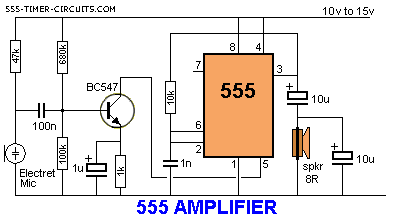
Power LED Driver Circuit Diagram

As you can see from the circuit diagram, the author chose an LT3518 switching regulator IC, which is a buck/boost converter optimised for LED operation. Here it is used as a down converter (buck mode). This IC can achieve better than 90% efficiency in this mode, depending on the input voltage. According to the typical application circuit on the data sheet [1], its switching frequency can be set to approximately 170 kHz by selecting a value of 82 kΩ for R1. To maximise overall efficiency with this type of IC, the volt-age drop over the sense resistor used to measure the current flowing through the LED should be as low as possible. This particular device operates with a voltage drop of 100 mV, corresponding to a current of just under 1.5 A with the specified value of 68 mΩ for R2. This value proved to be suitable for the Cree LED used by the author. At this current level, a diode with a power rating of at least 6 W should be used for D1.

IC1 has an additional property that is ideal for this application: the connect-ed LED can be dimmed by applying a PWM signal to pin 7 of the IC, with the brightness depending on the duty cycle. Obviously, the PWM frequency must be lower than the switching frequency. The PWM signal is provided by IC2, a special voltage-controlled PWM generator (type LTC6992 [2]). The duty cycle is controlled by the volt-age applied to the MOD input on pin1 (range 0–1 V). The resistor connected to pin 3 determines the internal clock frequency of the IC according to the formula f= 1 MHz × (50 kΩ/R3). This yields a frequency of approximately 73.5 kHz with R3 set to 680 kΩ, which is much too high for controlling IC1.

However, the PWM IC has an internal frequency divider with a division factor controlled by the voltage applied to pin 4, which in this circuit is taken from voltage divider R4/R5. The division factor can be adjusted over the range of 1 to 16,384. The division factor with the specified component values is 64, resulting in a PWM frequency of around 1,150 Hz. If you want to be able to generate a PWM signal with an adjust-able duty cycle over the full range of 0 to 100%, you must use the LTC6992-1 option. The -4 option, which provides a range from 5 to 100%, might be an acceptable alternative.To prevent the duty cycle (and thus the brightness of the LED) from depending on the battery voltage, which gradually drops as the battery discharges, IC3 generates a stabilised 1.24 V control voltage for potentiometer P1. Series resistor R7 reduces the voltage over P1 to 1V, which exactly matches the input voltage range of the LTC6992.

All capacitors should preferably be ceramic types, in particular due to their low effective series resistance (ESR) as well as other favourable characteristics. However, only capacitors with X5R or X7R dielectric should be used; capacitors with type Y dielectric have very poor temperature characteristics.The supply voltage is limited to 5.5V by the maximum rated supply voltage of IC2. The author used four NiMH re-chargeable cells connected in series, which yields a voltage that is just within spec. With an operating voltage in the range of 4.5 V to 5.5 V, you must use an LED that can operate at less than 4V.

This eliminates devices with several chips connected in series on a carrier, which is very often the case with power LEDS rated at over 5 W. These devices require a correspondingly higher supply voltage, which means more cells connected in series. This is only possible if the supply voltage for IC2 is reduced by a 5 V voltage regulator or other means, and of course R4 must also be connected to this lower supply voltage.

Finally, a few words about soldering. An exposed thermal pad must be provided on the PCB for the LT3518, and the rear face of the IC must be soldered to this pad. The author obtained good results by dimensioning the exposed pad large enough to extend beyond the outline of the IC. When assembling the board, first tin the pad and the rear face of the IC. Then heat the pad with a soldering iron. When the solder melts, withdraw the tip of the soldering iron to the edge of the pad and simultaneously place the IC on the pad and align it. After this the pins can be soldered.

Wireless LED Driver

There are times when you want to control a LED indicator light through the side of a plastic box, without wires and without drilling a hole in the box.  One example where this may be needed is in data collection systems.  These are often used out of doors in harsh environments and have to be hermetically sealed. Holes drilled in the side of the box for panel mounted LEDs or light pipes can often leak.

The circuit below solves this problem by sending power to the LED through the plastic, using a magnetic coupling technique. The circuit below can route power through plastic enclosures as thick as ¼ inch.  The circuit will not work through metal boxes.  An expensive inductor, driven by a series resonant mode 125KHz oscillator, forms the power transmitter.  A similar inductor, wired as a 125KHz parallel resonant circuit, forms the power receiver.  A voltage doubler circuit at the receiver efficiently converts the collected AC into DC.  The circuit will operate over a wide 3v to 6v supply range.

With a 5v supply, the circuit draws about 25ma of current.  However, by gating the oscillator on for a brief 20ms period, with a 0.5Hz rate, the average power can be reduced to about 250 microamps.  If you want to extend the range of operation out to ½ inch, try using a 74C14 (CD4069) with a 12v supply.  Using surface mounted components; the complete LED assembly can be encapsulated and glued to the outside surface of the box.  Tiny unshielded surface mounted inductors can be used to reduce the size of the transmitter and receiver.  However, smaller parts will reduce the power transfer range to perhaps only a 1/8 inch separation. 

A very nice bright green LED, which works great for this circuit, is one from Kingbright, available from Digikey, part number 754-1089-1. 

Light Sensitive and Differential Temperature Switch

n Fig. 1 see a precision light- sensitive switch that activates when the sensed quantities go above or below pre-set values. The LDR can be any cadmium sulfide unit that has a resistance in the range 500R to 20k at the required trip level. The RV1 adjust LDR at normal light level. 
Fig. 2 Differential Temperature Switch Circuit Diagram:
In Fig. 2 see a differential temperature switch circuit using ordinary silicon diodes as temperature sensing elements and responding to differentials of a fraction of degree. RV2 can be used to apply an effective offset of several degrees to the two diodes. To adjust the circuit, apply the required differential temperature to the diodes and then adjust RV2 so that the relay just turns on. The circuit responds to the relative temperatures, rather than the absolute temperatures, of the two diodes. 
Part List :
R1=LDR *see text 
R2-3=10Kohm 
R4=2.2Kohm 
R5-6-7-10=4.7Kohm 
R8-9=2.7Kohm 
RV1=22Kohm  pot. 
RV2=1Kohm  pot. 
D1-4=1N4001 
D3-4=1N4148 
Q1-2=BC214L 
IC1-2=LM741 
RL1-2=RELAY 12V >120 ohm

How to Build a Shake Tic Tac LED Torch

In the diagram, it looks like the coils sit on the “table” while the magnet has its edge on the table. This is just a diagram to show how the parts are connected. The coils actually sit flat against the slide (against the side of the magnet) as shown in the diagram:
The output voltage depends on how quickly the magnet passes from one end of the slide to the other. That's why a rapid shaking produces a higher voltage. You must get the end of the magnet to fully pass though the coil so the voltage will be a maximum. That’s why the slide extends past the coils at the top and bottom of the diagram.

The circuit consists of two 600-turn coils in series, driving a voltage doubler. Each coil produces a positive and negative pulse, each time the magnet passes from one end of the slide to the other. 

The positive pulse charges the top electrolytic via the top diode and the negative pulse charges the lower
electrolytic, via the lower diode.

The voltage across each electrolytic is combined to produce a voltage for the white LED. When the combined voltage is greater than 3.2v, the LED illuminates. The electrostatics help to keep the LED illuminated while the magnet starts to make another pass.


Tuesday, 28 January 2014

Sensitive Optical Burglar Alarm

This optical burglar alarm uses two 555 timer ICs (IC1 and IC2). Both the ICs are wired as astable multivibrators. The first astable multivibrator built around IC1 produces low frequencies, while the second astable multivibrator built around IC2 produces audio frequencies.
General-purpose Darlington photo-transistor T1 is used as the light sensor. To increase the sensitivity of the circuit, NPN transistor T2 is used.
Place phototransistor T1 where light falls on it continuously. Phototransistor T1 receives light to provide base voltage to transistor T2. As a result, transistor T2 conduct to keep reset pin 4 of IC1 at low level. This disables the first multivibrator (IC1) and hence the second multivibrator (IC2) also remains reset so the alarm (LS1) does not sound.
When light falling on Darlington phototransistor T1 is obstructed, transistor T2 stops conducting and reset pin 4 of IC1 goes high. This enables the first multivibrator (IC1) and hence also the second multivibrator (IC2). As a result, a beep tone is heard from speaker LS1. The beep rate can be varied by using preset VR1, while the output frequency of IC2 can be varied by using another preset VR2.
This circuit works off a simple 6V-12V DC power supply.
PARTS LIST
Resistors (all ¼-watt, ± 5% Carbon unless stated otherwise)
R1, R5 = 1 KΩ
R2 = 100 KΩ
R3 = 4.7 KΩ
R4 = 10 KΩ
VR1 = 1 MΩ
VR2 = 100 KΩ
Capacitors
C1 = 1 µF/16V
C2 = 0.01 µF
C3 = 0.047 µF
C4 = 0.01 µF
C5 = 47 µF/25V
Semiconductors
IC1, IC2 = NE555
T1 = 2N5777 Photo Transistor
T2 = BC547
LED1 = RED LED
Miscellaneous
LS1 = 8Ω / 0.5W

Monday, 27 January 2014

1.5V 555 LED Driver Experiment

This 1.5V 555 LED driver is more of a fun learning experiment than a practical circuit. While the TLC555 can indeed drive a 3V white LED using the inductive discharge technique, it typifies the kind of problems present in low voltage circuits. Two circuits are presented: Basic 555 LED Driver and Bootstrapped 555 LED Driver.
Circuit function

When the output (pin 7) goes low, it charges L1 and when it turns off, the voltage developed by the inductor discharge easily causes the voltage across the LED to increase to its threshold voltage and subsequently flow through the LED.

Bootstrap mode

Note that operation of the toggle switch is necessary to shock the device into oscillation at marginally low voltages – otherwise, it cannot start. What happens is that when the switch closes, C2 charges through L1 and rings up double the incident input voltage – this is the effect of series resonance. Rectifier D2 and capacitor C2 then hold Vcc at a higher voltage level until oscillation commences and L1 starts repetitively firing the LED at 3V thus keeping C2 charged. This is a very interesting part of the experiment.

Not all 555s are created equal

To make this LED driver circuit function, the 555 must operate well below the specified minimum Vcc. Also, the maximum voltage specification of the open collector output (pin 7, discharge function) is not specified in relation to Vcc (pin 8). The first TLC555 worked so poorly under these conditions that I decided not to use its data. The particular LM555 was selected because I knew that it functioned OK at very low voltages. So a word for the wise – whoever attempts to replicate any of this stuff, will need a bag of 555s.

Results, Fig 1

Minimum voltage TLC555: 1.36V (some LED current as low as 1.0V – self-starting @ 1.0V)
Minimum voltage LM555: 2.30V (no LED current below this point – self-starting @ 2.3V)

Results, Fig 2, bootstrap mode

Minimum voltage TLC555: 1.13V (some LED current as low as 0.56V, self-starting @ 1.1V)
Minimum voltage LM555: 1.78V (some LED current as low as 0.80V, self-starting @ 2.5V)

Datasheet ZXSC380 (for comparison – I did not actually test this device)

Minimum startup and operating voltage: 0.9V typical, 1.0V max

Muting Transistor Attenuator Circuits and the 2SC2878

Among semiconductors, the muting transistor and its audio application is perhaps the most obscure and poorly understood of all. There is extremely little information on this subject available on the internet and what is available is sketchy. This discussion is an attempt to tie the pieces together and to add some insight –I have been working on this off and on for some time and for me it has been a learning experience. While I do not claim expertise in this subject, I question if such experts actually exist.
Applications for muting circuits
Applications for muting circuits abound. Included are synthesizers, audio amplifiers, pre-amplifiers, audio mixers and audio line & level equipment (both consumer and professional). In amplifiers and pre-amplifiers, the muting circuit is intended to prevent the popping of loudspeakers when power is applied. In mixers and audio line & level equipment, the muting circuit may also be employed to select /deselect various input channels –such must be done cleanly or quietly.
Types of muting circuits
Obviously, the function of muting circuits is to mute (kill) the audio signal. This can be done in a number of ways including switches, relay contacts, junction FETs, analog switches and bipolar muting transistors. Switch and relay contacts can be noisy and intermittent due to contact bounce. Furthermore, properly applied contacts must be dry circuit rated due to both the low current and potential across the contacts –this forces the use of bifurcated dry circuit contacts that are special and expensive. While a junction FET is sometimes applied as a variable attenuator, its use as a muting device is a misapplication due to the lack of symmetry because it cannot support more than about 600mV due to its intrinsic body diode. Analog switches can do the job if applied correctly, but lack the audio range required in professional line and level applications, may be subject to crosstalk between sections and are also very sensitive to ESD. On the other hand, the bipolar muting transistor does everything well and inexpensively.
What is unique about the bipolar muting transistor?
The standard NPN transistors is symmetrical in that it consists of 3 layers, 2 layers of “N” material (collector & emitter) separated by a layer of “P” material (base). However, that is as far as the symmetry goes as the layer thicknesses and doping varies greatly. The standard transistor still functions with the collector and emitter terminals reversed, but the hFE (current gain) in this mode is reduced by perhaps two orders of magnitude and the reversed voltage rating (Vebo) generally limited to about 5V.
In comparison, the muting transistor is a good deal more symmetrical –it has high reverse hFE and some types offer a 15 to 40V base to emitter reverse voltage rating (Vbeo). In effect, it is rated for AC operation and this suits it well for audio voltage signals that are AC in nature. Whichever terminal (emitter or collector) is the most negative becomes the effective emitter terminal. If sufficient base drive is applied, it will saturate either polarity, and this is exactly what is required to implement the mute function.
Two categories of muting transistors
The two categories are graded by the base to emitter reverse voltage rating (Vbeo).
The 1st category Vbeo is limited to 5V and is suited for consumer electronics that has an average program signal level of -7.8dbu (0.315Vrms or 0.445Vpeak). A 5V rated device provides 21db headroom to handle program material transients.
The 2nd category Vbeo starts at 15V and is suited for professional studio line and level devices that have an average program signal level of +4dbu (1.228Vrms or 1.736Vpeak). A 15V rated device provides 18.7db headroom to handle program material transients.

BBC NEWS

ARY NEWS


Sunday, 26 January 2014

NATIONAL GEOGRAPHIC


GEO NEWS


WATCH


555 Amplifier Circuit

The 555 can be used as an amplifier. It operates very similar to pulse-width modulation. The component values cause the 555 to oscillate at approx 66kHz and the speaker does not respond to this high frequency.  Instead it responds to the average CD value of the modulated output and demonstrates the concept of pulse-width modulation. The chip gets very hot and is only for brief demonstrations. 

Knight Rider Circuit


Inverted 555 Timer Circuit

Whenever I use the 555 timer, it seems that the output polarity is invariably incorrect, and the way the 555 functions, it normally cannot generate a duty cycle of less than 50% — 90% yes, 10% NO! This inverted 555 circuit generates duty cycles of less than 50%. Everything works the same except for the polarity. Why not simply invert the output with a transistor? Will not that do the same? Legitimate question… Actually NO, because a transistor that inverts the output cannot provide the desirable totem pole source/sink output function of pin 3. And there is another reason that we will get in the future—this is a 555VCO circuit that requires the inverted timer.
The schematic shows (3) circuits, because one circuit does not work well over the entire Vcc range.
The first simply uses a “normal” 2N3904 garden variety transistor, and this works well when Vcc < 9V. When Vcc > 9V, the base to emitter junction starts to zener and disrupts operation. Transistor base to emitter junction zeners a little above -6V.
The second circuit adds D1 to the emitter of Q1 in order to increase VEBO. With this mod, Vcc may be increased to the 18V limit. However, D1 may be eliminated if we use the special 2SC2878 switching transistor that has a VBEO rating of -25V. These devices are no longer in production, but are available on eBay—every serious experimenter should have a few in his component collection. The types now in production use the tiny SO-23 SMD package.
The third circuit uses a J112 N-Channel JFET for Q1. The JFET is a curious device that works well for the application provided we allow for the VGS(OFF) parameter. VGS must be less than Vcc /3. (e.g. if Vcc = 9V, VGS(OFF) must be less than 9V /3 or 3V for proper operation). Since the VGS(OFF) parameter is sloppy (-1 to -5V), the device must be selected—to the left is a simple test circuit—actually, most devices will work OK. The J112 should also be in every serious experimenter’s component collection.
How it works
You will note that C1 is tied to Vcc rather than common and that R1 & R2 charge it in the negative direction. By connecting C1 to Vcc, the relatively high discharge current does not run through the power source. The reset transistor (Q1) discharges the capacitor in the positive direction. R1 & R2 are determined in the same fashion as the normal 555 timer. R3 is a pull-up resistor for the open collector output (pin 7) so it can drive the emitter follower (or source follower) reset transistor.
R1 scales the output frequency—here it is about 1.25kHZ and it can be rescaled to whatever you need.
R2 controls the reset pulse width for low duty cycle (short output pulse) output—the larger it gets, the more it affects output frequency.
Pin 5 does not need a bypass capacitor unless you desire high stability generally I omit this capacitor.

Temperature Alarm Circuit

This simple Over heat alarm is to monitor heat generating devices such as motor, inverter etc. The alarm will beep and LED blinks when the temperature of the device increases abnormally.
The circuit is a simple Astable multivibrator using the low power CMOS timer IC 7555 which is the low power version of the popular 555 IC. The reset pin 4 of IC1 is used to activate the alarm. The astable will work only if the reset pin 4 becomes high. The reset pin is connected to the positive rail through the 10 K NTC thermister. The NTC (Negative Temperature Coefficient) thermister offers high resistance in cold and its resistance becomes low to few ohms when the temperature in its vicinity increases. So when the temperature is low (as adjusted by the position of the thermister near the device) reset pin of IC1 remains low and astable is in off position and buzzer remains silent. When the temperature near the thermister increases, its resistance decreases and provides voltage to the reset pin of IC1 and the astable starts working.
Note: Fix the thermister near the device by adjusting the distance between the thermister and the heat generating area of the device so as to keep the alarm silent when the heat is normal.


Digital signal processing (DSP) Practical


EMBEDDED SYSTEM

Embedded systems
Examples of Embedded systems
Technology for Embedded systems
Microprocessor vs Microcontrollers
Microcontroller Families
Criteria to choose a microcontroller
Overview of 8051 family
Applications/ Some projects

TRW&PS

Important Presentation Characteristics
• Purpose
o Be clear about the message that you are trying to convey.
• Audience
o Know your audience and their level of understanding.
o Make your presentation appropriate to their interests & level of
understanding.
o Make it interesting.
• Approach
o Make it easy for your audience to agree with your message.
• Time Limit
o Do not exceed the time limit.
o To know how long your presentation will run you must practice.
o Do not move any faster than one slide per minute.

Sunday, 12 January 2014

Learning Physics Modeling with PhysX


Book Description
In this day and age, physics engines play a very critical role in the success of a sophisticated game. PhysX is a state-of-the-art cross-platform physics engine widely used by top game studios and developers. It contains all the physics-related components you will need and exploits the parallel-processing capability of modern GPUs as well as multi-core CPUs to make a game as physically-realistic as possible. This book will help you to program and simulate games by using PhysX 3.

Learning Physics Modeling with PhysX helps you to master physics simulation using the PhysX Physics Engine from scratch. This is useful not only for game developers, but also for developers making virtual walkthroughs or training and other simulation applications. It will cover all the essential features of PhysX 3 with easy-to-understand code snippets and examples to help you learn quickly and efficiently.
Book Details
Publisher: Packt Publishing
By: Krishna Kumar
ISBN: 978-1-84969-814-6
Year: 2013
Pages: 104
Language: English
File size: 3.7 MB
File format: PDF

A Peek at Computer Electronics


Book Description
Are you a programmer or computer enthusiast? Do you feel comfortable with methods, functions, and variables? Do you wish you knew more about how the computer made it all work? Now you can. From basic electronics to advanced computer hardware, you'll learn the magic behind the gear that makes it all run.

If you're into tinkering, or ever thought about it, this book explains the basics of how it all works.
Book Details
Publisher: The Pragmatic Programmers
By: Caleb Tennis
ISBN: 978-0-9776-1668-8
Year: 2007
Pages: 250
Language: English
File size: 5.52 MB
File format: PDF